
In a groundbreaking discovery, researchers at Imec have successfully grown lasers directly on silicon, paving the way for cost-effective, high-performance optical devices.
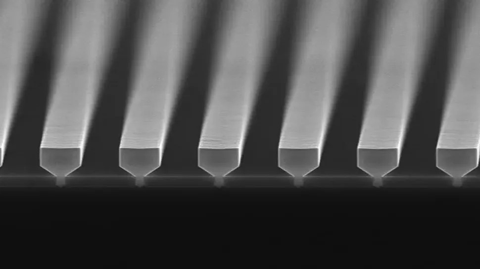
This innovative achievement uses gallium arsenide, a material that doesn’t naturally bond with silicon, to create high-quality lasers. The process involves covering a silicon wafer with a layer of silicon dioxide and etching arrowhead-shaped trenches. Gallium arsenide is then deposited into these trenches, where it makes contact with silicon only at the bottom, minimizing defects.
Room-Temperature Lasing Achieved
The lasers have achieved room-temperature continuous-wave lasing with threshold currents as low as 5 mA and output powers exceeding 1 mW. This breakthrough has significant implications for the development of high-performance optical devices, particularly in data communications, machine learning, and artificial intelligence.
What Does This Mean for the Future of Technology?
The ability to grow lasers directly on silicon reduces the need for expensive III-V substrates and complex bonding processes, making it a cost-effective solution. The scalability of the fabrication process, compatible with standard 300 mm silicon wafers, enables large-scale production.
Imec’s breakthrough is a significant step forward in the development of high-performance optical devices. As the demand for faster, more efficient technology continues to grow, this innovation is poised to play a critical role in shaping the future of data communications and beyond.
Stay tuned for further updates on this exciting development!


